Quick build
Build your own Core8Bit in one evening. It is free for your own build. Want to sell consoles you build? You can, read the rules. This page only says what goes where and what connects to what. When you need more detail, the full build guide has it.
There are two ways to build it:
| A. Wired | B. Mainboard | |
|---|---|---|
| What holds the modules | a 3D-printed base plate | a home-made PCB of the same shape |
| How they connect | wires | tracks on the board |
| Status | works today | ready for CNC-milled boards |
Safety. Solder only with the battery disconnected. Check battery polarity twice. Do not heat the battery.
What you need
- Parts: the parts list (core board, 4.3" screen, ESP32, two 5 V boost modules, 21 V backlight booster, charger board, Li-Po 606090, PAM8406 amplifier, 2 speakers, 2 sticks, 10 buttons, microSD).
- Tools: soldering iron, multimeter, a 3D printer (or a printing service).
- Firmware: flashed from the flash page in your browser.
A. Wired build
1. Print the case
Download the case files (zip) and print them: PLA or PETG, 0.2 mm layers. Free for your own build: one click to accept the agreement before the first download. The speaker enclosures are sold separately on our itch.io page.
| File | Part |
|---|---|
case-top.stl |
front of the case |
case-back.stl |
back cover |
base-plate.stl |
base plate: holds the buttons and sticks in front, the modules behind |
screen-frame.stl |
holds the screen and the battery |
spk-L.stl, spk-R.stl |
speaker enclosures (itch.io, not in the zip) |
2. Flash before you assemble
Open the flash page in Chrome or Edge and follow it. It flashes both chips over USB, no programmer and no software needed:
- Console (STM32): hold BOOT0, plug in the core board's USB port, click Flash console.
- Wi-Fi module (ESP32): plug in its USB-C, click Flash Wi-Fi module.
- SD card: format FAT32 and copy the system files onto it.
3. Put everything on the base plate
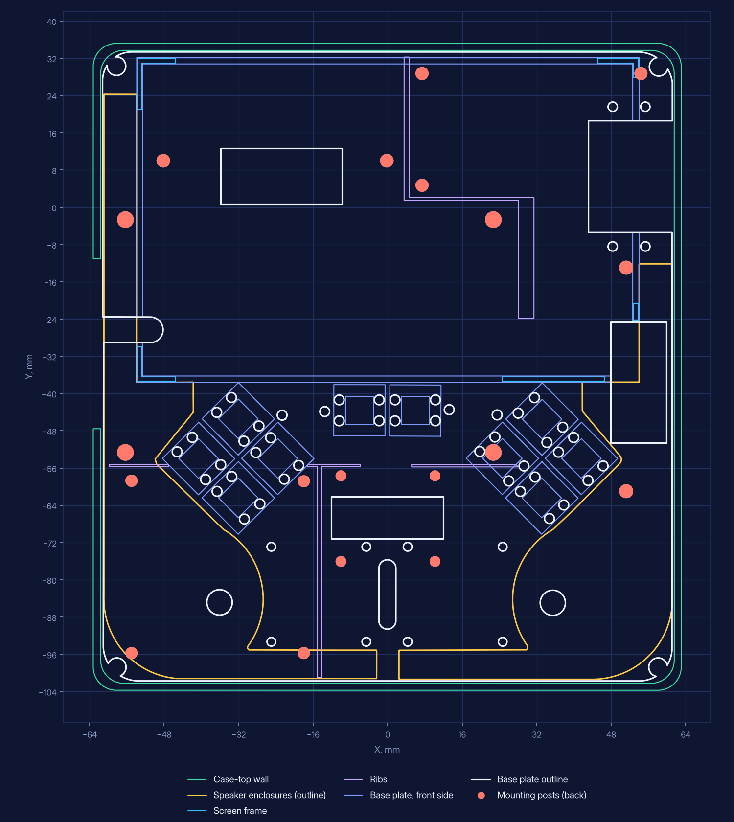
Front side:
- D-pad on the left, A/B/X/Y on the right, MENU and SELECT in the middle (button legs into the holes).
- Two sticks at the bottom.
- The screen goes into the screen frame, the battery behind the screen.
Back side (modules sit on the posts of the base plate, glue comes later):
- core board in the centre, SD slot reachable;
- ESP32 at the top, its USB-C at the right edge (looking at the screen);
- two FFC adapters: one next to the core board, one at the screen ribbon;
- amplifier in the middle, under the window for its volume knobs;
- charger and boosts at the bottom left.
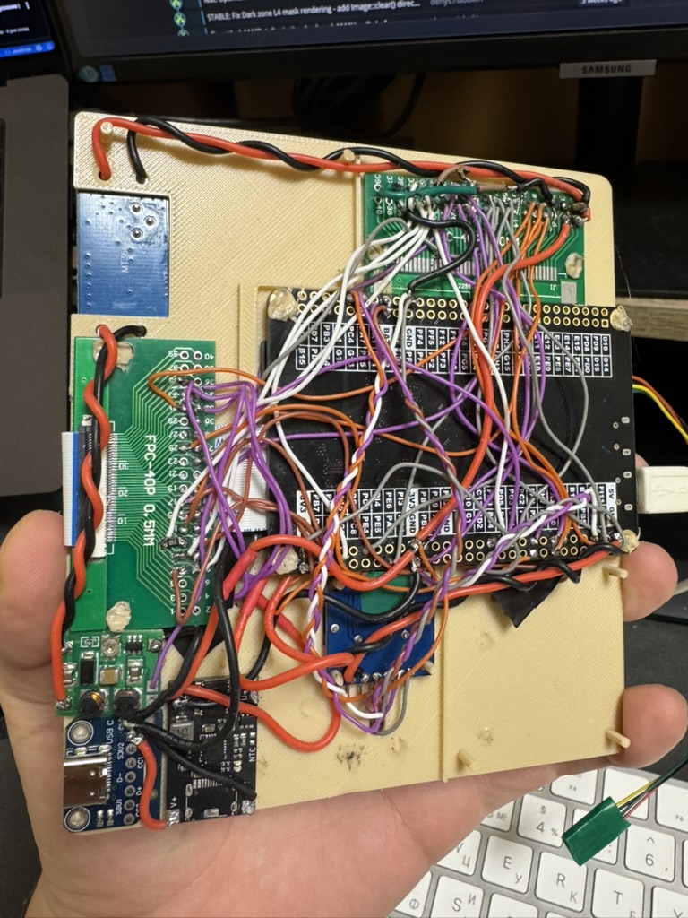
4. Wire it
Names like R12.1 are positions on the core board headers (right block, position 12, row 1). contact n is a pad on an FFC adapter.
Screen
The ribbon goes from the core board's "LCD interface" connector to the first adapter. Most screen lines come from there, the rest from the headers. Each line ends on the screen-side adapter.
Each adapter folds the ribbon, which reverses the pin order. Always connect by signal name, not by pad number.
| Signal | From the core board | To screen-side adapter contact |
|---|---|---|
| CLK | board-side adapter contact 30, through 33 Ω | 11 |
| HSYNC | R26.2, through 33 Ω | 9 |
| VSYNC | board-side adapter contact 32, through 33 Ω | 8 |
| DE | board-side adapter contact 33, through 33 Ω | 7 |
| DISP | R12.1 | 10 |
| R3 · R4 · R5 · R6 · R7 | R7.2 · contact 16 · R3.2 · R6.1 · contact 10 | 33 · 32 · 31 · 30 · 29 |
| G2 · G3 · G4 · G5 · G6 · G7 | R22.2 · R24.1 · R2.2 · contact 17 · R2.1 · R13.1 | 26 · 25 · 24 · 23 · 22 · 21 |
| B3 · B4 · B5 · B6 · B7 | contact 24 · contact 25 · R7.1 · R19.2 · R19.1 | 17 · 16 · 15 · 14 · 13 |
| 3.3 V | R20.1 | 37 |
| GND | GND | 38, 12, 5 and the unused colour bits 36–34, 28–27, 20–18 |
| Backlight + / − | 21 V booster output + / − | 39 / 40 |
Leave board-side adapter contact 40 free. Wrap the ribbon and both adapters in foil tape over Kapton and connect the foil to GND.
Buttons
Every button connects its pin to 3.3 V when pressed (never to GND). One common 3.3 V wire goes to all buttons, plus one wire per button:
| UP | DOWN | LEFT | RIGHT | A | B | X | Y | MENU | SELECT |
|---|---|---|---|---|---|---|---|---|---|
| contact 31 | contact 27 | contact 28 | R8.2 | contact 6 | contact 7 | contact 8 | contact 9 | R9.2 | contact 26 |
Sticks
Each stick axis: ends to 3.3 V and GND, middle pin to the core board.
| Right X | Right Y | Left X | Left Y |
|---|---|---|---|
| L22.2 | L24.1 | L23.2 | L25.1 |
ESP32
| ESP32 pin | Core board | Note |
|---|---|---|
| GND | R17.2 | |
| VIN | 5 V from boost #1 | |
| D18 | R17.1 | 33 Ω at the core board |
| D23 | R22.1 | 33 Ω at the core board |
| D19 | R23.2 | 33 Ω at the ESP32 |
| D5 | R14.2 | 33 Ω at the core board, plus 10 kΩ from D5 to 3.3 V |
| D4 | R13.2 |
Power
battery ─► charger board ─┬─► boost #2 ─► ferrite bead ─► 5 V to the core board
                          └─► boost #1 ─► ferrite bead ─► 5 V to ESP32, amplifier, 21 V booster
                              EN ◄─ R24.2, plus 100 kΩ from EN to GND
Set both boosts to 5.0–5.1 V and the 21 V booster to about 19 V before you connect anything.
Sound
| From | To |
|---|---|
| R9.1 (left) · R3.1 (right) | amplifier LIN · RIN |
| core board GND | amplifier input GND (twist it with the two signal wires) |
| 5 V from boost #1 | amplifier VCC / GND |
| amplifier LOUT+ / LOUT− · ROUT+ / ROUT− | left speaker · right speaker (never connect the − outputs to GND) |
Interference on the wired build
Loose wires pick up noise. You may see it on the screen (the picture drifts, rows of wrong pixels crawl across it) or hear it in the speakers (hiss or rustle when nothing plays). To prevent it:
- Tape the solder joints on both FFC adapters and the screen connector with Kapton or electrical tape.
- Wrap foil over the tape: the ribbon, both adapters and the screen wires.
- Ground the foil: one wire from the foil to GND at one point.
- Keep the screen and sound wires away from the boost modules and the 21 V booster.
- Twist each sound wire with its ground wire, and the speaker wires in pairs.
- If the picture still jitters, use 47 Ω instead of 33 Ω on CLK, HSYNC, VSYNC and DE.
Keep the foil away from the ESP32 antenna (the end of the module with the zigzag track). The mainboard build does not need any of this: its ground layer does the job.
5. Close the case
- Glass, then screen, then battery into the screen frame.
- Speakers into the speaker enclosures, tight, with no air gaps.
- Into the case front: speaker enclosures, screen frame, base plate.
- Power on once before closing (next step).
- Back cover on, 4 corner screws.
6. First power-on
- Measure both boost outputs: 5.0–5.1 V. Core board 3.3 V pin: 3.25–3.35 V.
- Power on: the boot screen appears and the launcher shows the games.
- SELECT → Settings → Sticks: calibrate the sticks.
- SELECT → Settings → WiFi: connect to your network.
Something not working? See troubleshooting.
B. Mainboard build
Prefer pictures? Building on the mainboard shows every step in two views, one module at a time.
The mainboard replaces the base plate and all the wires: every module plugs into it on pin headers. This version (v0.5) is made for CNC isolation milling at home: a 2-layer board, no plating, vias made from thin wire.
1. Get the files
Download (free for your own build, one click to accept the agreement before the first download):
| File | What it is |
|---|---|
| Board, Gerber + drill (zip) | copper top and bottom, outline, drill files |
| Board, mirrored for the bottom side (zip) | the same, mirrored about x = 0, for milling the back |
| KiCad project (zip) | open it in KiCad 7 or newer |
| Screen frame for the mainboard (STL) | the screen frame with melt pins that go through the board |
Print case-top, case-back from the case files. You do not need base-plate.stl or the wired screen-frame.stl.
2. Mill the board
You need a CNC with a 20° / 0.1 mm V-bit, a 0.6, 0.9 and 1.0 mm drill, a 1.0 mm end mill and height-map levelling (Candle, bCNC or FlatCAM autolevel). FR-4 1.6 mm, copper on both sides, blank 125 × 140 mm.
| Setting | Value |
|---|---|
| Isolation | V-bit 20°, tip 0.1 mm, depth −0.08 mm, 2 passes, 15–20 % overlap (about 0.3 mm isolation) |
| Height map | grid 8 mm, on each side before milling |
| Drills | 0.6 (vias), 0.9 (buttons), 1.0 (headers); holes 2 mm and larger: mill with the 1.0 mm end mill |
| Outline | 1.0 mm end mill, depth −1.7 mm, 0.6 mm per pass, 4 tabs |
| Flip axis | x = 0 (vertical), left to right |
- Drill the three registration holes REG1 (0, −14), REG2 (0, −32), REG3 (0, −97) with a 3.0 mm drill through the blank into the spoil board and insert 3 mm pins. Their uneven spacing lets the board sit on the pins only one way.
- Height map, then mill the top copper.
- Drill all holes.
- Flip the board left to right onto the pins. Height map, then mill the bottom copper (use the mirrored files, or the normal bottom file with mirror axis x = 0).
- Cut the outline. Clean the board, check for shorts between neighbouring tracks with a multimeter.
3. Make the vias
The holes are not plated, so every via is a short piece of 0.6–0.7 mm tinned copper wire: push it through, solder it on both sides, cut it flush. Do all vias before any parts. The via map (PNG) shows each one.

4. Solder the small parts
Parts go where the silkscreen shows them. All resistors and capacitors are 0805 unless noted.
| Qty | Value | Where |
|---|---|---|
| 8 | 33 Ω | R1–R4 (screen CLK, HSYNC, VSYNC, DE), R40–R43 (ESP32 SPI) |
| 2 | 1 kΩ | R5, R12 |
| 5 | 10 kΩ | R6, R7, R13, R14, R33 |
| 4 | 100 kΩ | R8, R15, R16 (boost #1 EN pull-down), R35 |
| 1 each | 22 kΩ R32, 100 Ω R34, 330 Ω R36 | |
| 2 | 0 Ω | R37 (0805), R38 (1206) |
| 5 | 1 µF | C2, C4, C5, C9, C10 |
| 2 | 10 nF | C3, C8 |
| 1 | 100 nF | C14 |
| 3 | 22 µF 1206 | C11, C12, C13 |
| 1 | 220 µF 10 V electrolytic | C1 |
| 3 | ferrite bead ≥ 2 A | FB1, FB2 (1206), FB3 (0805) |
| 1 | SS34 diode (SMA) | D2 |
| 1 | BAS16 (SOT-23) | D3 |
| 1 | LED 0805 | D4 |
| 1 | AO3400A (SOT-23) | Q8 |
| 1 | PTC fuse 1.5 A 1206 | F1 |
Leave R31 and R39 empty. SB1 is a closed solder bridge: leave it closed.
5. Buttons and sticks
Ten tact buttons (D-pad, A/B/X/Y, MENU, SELECT) and the reset button go on the front side; solder their legs on the back. The two sticks plug into J5 (left) and J6 (right): 1 GND, 2 3.3 V, 3 X, 4 Y.
6. Modules
All modules sit on the back of the board on pin headers. Solder their pins on the front side.
- Core board: long pin headers (11.5 mm), chips facing the mainboard, on the plastic spacers. Its micro-USB points at the slot in the left wall. Clip the long pins flush on the screen side and cover them with Kapton tape (the battery lies there). Trim the short side to 1 mm or less.
- ESP32: chips facing out. Its corner hole sits on the corner screw of the case, its USB-C at the right wall.
- FFC adapters: on J3 (next to the core board) and J4 (at the screen ribbon). Their sockets sit in the board windows.
- Power and sound modules:
| Header | Module | Pins |
|---|---|---|
| J13 | charger | 1 IN, 2 GND, 5 OUT (to the switch), 6 GND, 7 status. Battery wires go through the oval hole straight to the charger's B+ / B− |
| J14 | power switch | 1 to the boosts, 2 from the charger |
| J15 | boost #2 (core board, always on) | 1 IN+, 2 IN−, 3 OUT+, 4 OUT− |
| J16 | boost #1 (switched 5 V) | 1 IN+, 2 IN−, 3 OUT+, 4 OUT−, 5 EN |
| J17 | 21 V backlight booster | 1 IN+ (5 V), 2 GND, 3 LED+, 4 LED− |
| J7, J8 | PAM8406 amplifier | J7: 5 GND, 6 VCC. J8: 1 left in, 2 audio GND, 3 right in |
| J11 | VS1003B MP3 module (optional) | as printed on the board |
| J18 | 5 V from the core board's micro-USB, for charging | 1 VBUS, 2 GND |
| J22, J23, J24 | microphone, expansion, vibration motor (optional) | as printed on the board |
Set both boosts to 5.0–5.1 V and the backlight booster to about 19 V before you plug in the core board and the screen.
7. Speakers, screen and case
- Speakers into their enclosures. Run each speaker's wires through the two small holes next to it and solder them to the amplifier outputs (never connect the − outputs to GND).
- Glass, screen and battery into the screen frame. Push the frame's pins through the holes in the board and melt their ends flat on the back with the soldering iron (the four thin pins in the bottom-left corner melt together into one plate). Glue the other frame supports with super glue or double-sided tape.
- Connect the screen ribbon to the J4 adapter.
- Flash, power on and close the case as in A: step 2, step 6, then step 5.
The board's ground layer shields the screen and sound lines, so the foil and extra ground wires of the wired build are not needed.